Unpacking Xilinx 7-Series Bitstreams: Part 1
For the past few months, I’ve been writing Xilinx 7-series bitstream manipulation tools for SymbiFlow. After building a mostly-working implementation in C++, I started to wonder what a generic framework for FPGA development tools would look like. Inspired by LLVM and partly as an excuse to learn Rust, I started a new project, Gaffe, to prototype ideas. With Xilinx 7-series fresh in my mind, I chose to reimplement the bitstream parsing as a first step. While most of the bitstream format is documented in UG470 7 Series FPGA Configuration User Guide, subtle details are omitted that I hope to clarify here.
File Formats Galore
Xilinx 7-series devices can be programmed through multiple interfaces (JTAG, SPI, BPI, SelectMAP) and multiple tools (iMPACT, SPI programmer, SVF player). This has led to multiple file formats being devised for different scenarios:
- BIT
- Binary file containing BIT header followed by raw bitstream
- RBT
- ASCII file with text header followed by raw bitstream written as literal ‘0’ and ‘1’ characters for each bit
- BIN
- Raw bitstream
- MCS
- PROM file format (includes address and checksum info)
Even though a BIN contains all the necessary data for programming a part, BIT is the default format generated by Vivado’s write_bitstream command and is what I’ll focus on.
BIT Header
Thankfully, this header format was documented on FPGA FAQ back in 2001. It’s mostly a TLV format but with a few quirks. The information provided (design name, build date/time, target part name) are purely informational (ignored by the chip). The main reason I mention this format is that most other tools (Vivado, openocd) require this header to be present.
Layers of encapsulation
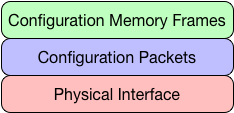
Past the BIT header, the raw bitstream is literally a stream of bytes that is interpreted by a 7-series part’s programming logic. Similar to networking protocols, part programming is built out of a protocol stack.

Starting at the base is the physical interface (JTAG, SPI, etc) used to connect to the part. The physical interface carries a packetized format that controls the overall programming operation through a series of register reads/writes. Part of the register set provides indexed access to the top layer of the stack: configuration memory frames.
Physical Interface Layer
As multiple physical interfaces are available, the electrical details depend on the specific interface you choose to use. The only common piece of the physical interface layer is the detection of a sync word (0xAA995566) that begins the parsing of packets.
Any data received prior to to the sync word will not parsed as a packet but may have other effects. For example, a few of the physical interfaces allow for multiple parallel bus widths. The interface hardware looks for a magic sequence, called the bit width detection pattern, to determine the width of the parallel interface. For details on how this works, see Chapter 5 of UG470.
Moving up the stack
In Part 2, I’ll be describing the packet format and the overall programming sequence. Part 3 will focus on configuration memory frame addressing and a few places where this careful encapsulation gets violated.